NIST Electron Physics Group Nanostructure Collection
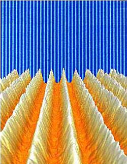 Laser-Focused Atomic Deposition. In this new form of nanofabrication, a laser standing wave propagates across a Si surface, concentrating atoms into its nodes as they deposit. Shown is a composite of two atomic force microscope images. The foreground is a three-dimensional rendering of an atomic force microscope image, showing 65 nm wide Cr lines. The background is a larger-range AFM image of the same sample, illustrating the regularity of the lines, which are spaced at exactly half the laser wavelength.
Reference: J.J. McClelland, R.E. Scholten, E.C. Palm, R.J. Celotta, Science 262, 877 (1993).
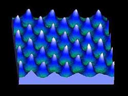 Laser-Focused Atomic Deposition of Nanodots. In this new form of nanofabrication, a laser standing wave propagates across a Si surface, concentrating atoms into its nodes as they deposit. Here, a two-dimensional standing wave creates an array of dots on the surface, spaced at exactly half the laser wavelength. The image is taken with an atomic force microscope on an array of Cr features on a Si surface. For this sample, the dots are spaced at 212.78 nm, and have height and width of 13 and 80 nm, respectively.
Reference: R. Gupta, J. J. McClelland, R. E. Scholten, Z. J. Jabbour, and R. J. Celotta, Appl. Phys. Lett. 67, 1378 (1995).
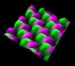 Colored Atoms in Compound Semiconductor Surfaces. Two superimposed STM imagesof the gallium arsenide (110) surface obtained at two different tunneling voltages. The green image shows the position of the gallium atoms obtained when electrons tunnel into the surface and sample the predominately empty gallium surface states. The red image shows the position of the arsenic atoms obtained when electrons tunnel from the surface into the tip and sample predominately filled arsenic surface states. The combined image reconstructs the whole surface of the gallium arsenide (110) surface
Reference: L. J. Whitman, J. A. Stroscio, R. A. Dragoset, and R. J. Celotta, unpublished
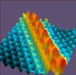 Self-Assembly of Atomic Wires. STM image showing zig-zag chain of cesium atoms (red) on a gallium arsenide (110) surface (blue). The image size is 7x7 nm. These atomic wires form naturally by self-assembly when cesium atoms are deposited on the GaAs surface. The self-assemble process results from cesium atoms diffusing on the surface and searching out the ends of existing cesium chains, which are preferential sticking sites.
Reference: L. J. Whitman, J. A. Stroscio, R. A. Dragoset, and R. J. Celotta, Phys. Rev. Lett. 66, 1338 (1991).
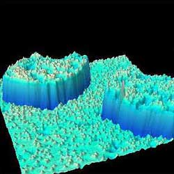 Atomic Scale Alloying. STM image, 35nm x 35nm, showing atomic scale alloying of chromium atoms (small yellow bumps) on an iron (001) surface when chromium atoms are deposited on the iron surface. The two islands are single atomic steps composed of iron atoms that were kicked out of the surface by the deposited chromium atoms. The islands also show alloyed chromium atoms. The chromium atoms reside in an iron lattice site and are a substitutional impurity. The chromium impurities at the iron-chromium interface have a significant effect on magnetic properties of films composed of layers of iron and chromium layers.
Reference: A. Davies, J. A. Stroscio, D. T. Pierce, and R. J. Celotta, Phys. Rev. Lett. 76, 4175 (1996).
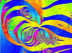 Domain Structure Near a Defect in an Amorphous Ferromagnet. The magnetic domain structure of an amorphous magnetic ribbon revealed by the technique of scanning electron microscopy with polarization analysis. The colors in this image correspond to different magnetization directions. This type of ribbon is commonly used in the magnetic core of power line transformers. Defects, such as the one in the center of this image, interact with the magnetic domain structure, interfering with the domain wall motion. These interactions result in energy losses that reduce transformer efficiencies.
Work done in collaboration with Allied Signal Corp. John Unguris, Electron Physics Group, NIST
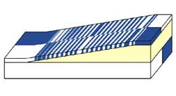 Magnetic Coupling in Fe/Cr/Fe. This figure shows the magnetic coupling between an Fe film and an Fe crystal separated by a wedge-shaped Cr spacer layer. The indirect coupling through the spacer switches from ferromagnetic (aligned Fe magnetizations) to antiferromagnetic (opposed magnetizations) with every single atom thick change in Cr layer thickness. The magnetic domain structure of the Fe film is imaged using scanning electron microscopy with polarization analysis, and it is shown superimposed on a schematic of the wedge structure. Black and white contrasts in the image correspond to opposite magnetization directions.
Reference: "Observation of Two Different Oscillation Periods in the Exchange Coupling of Fe/Cr/Fe(100)", J. Unguris, R.J. Celotta, and D.T. Pierce, Phys. Rev. Lett.. 67, 140 (1991)
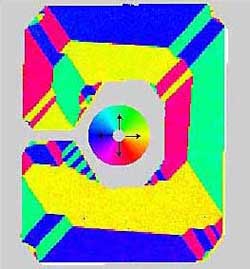 Patterned Magnetic Element. Scanning Electron Microscopy with Polarization (SEMPA) image of the magnetic domain structure of a patterned Fe thin film structure. This C-shaped structure, produced at the Naval Research Labs, is a prototype magnetic device for use in hybrid magnetoelectronic circuits. The element is 100 mm tall and about 50 nm thick. The direction of the magnetization is coded into color as given by the color wheel in the center of the image.
Reference: John Unguris, Electron Physics Group, NIST
