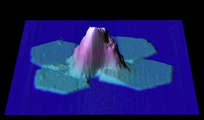
Lead Disulfide Microcrystals

Atomic force microscopy (AFM) image of lead disulfide microcrystals grown on a silicon oxide surface patterned by the AFM using "Dip-pen Nanolithography" (DPN). The field of view is 11.6 µm across, and the hexagonal crystallites are about 60 nm high. DPN was used to write a 5 µm x 5 µm chemically-reactive region on the wafer, which was then soaked in lead acetate and exposed to H2S gas. Microcrystals selectively grew starting from the patterned area.
S. E. Kooi, L. A. Baker, P. E. Sheehan, and L. J. Whitman.
Image courtesy: Dr. L. J. Whitman, Naval Research Laboratory.
